Technology area
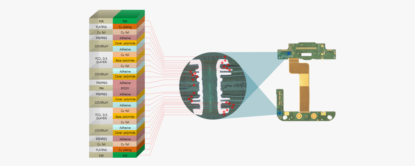
Structure of FPCB
Technology area
Structure of FPCB
Rigid FPCB
TECHNOLOGY DRIVEN ELECTRONIC COMPANY
- Build up
- Gloflex will become a company that continuously struggle and challenge toward the global best position with the core value and the core strategies.

Explanation
- Generic term of Via for build-up layer of build-up circuit board
- Build-up method builds up conductor layers by forming a conductor layer after a insulation layer, one by one; It allows to build VIA layers needed for each layer, mostly layering on both sides of the board one by one; applied for high density, highly integrated devices as it allows high speed signaling
- A specialized product applied for FPCB-Multi and RiGID-FPC products; allows to form more circuits than a same-sized product and realizes multi-function, high reliability and miniaturization
Main features
- A specialized product applied for FPCB-Multi and RiGID-FPC products; allows to form more circuits than a same-sized product and realizes multi-function, high reliability and miniaturization
- Applies mainly for connector cables and sub-boards; uses mainly supplementary boards for the soldering parts
- Realizes high density FPCB
- Compact design via a hidden VIA hole
Usage
- mobile module, LCD module, camera module ETC
- Wireless communication : Bluetooth
- Medical equipment /Military equipment
Specification
| ITEM | SPEC |
|---|---|
| Layers | 3~8 |
| Base Material | Polyimide or Polyester |
| Cover-lay | Polyimide or Polyester or Solder Mask |
| Thickness | 0.2mm~0.8mm |
| Line Width/Space | Normal Min, 0.07/0.07mm, Special Min. 0.06/0.06mm |
| Conductor | 1/3oz, 1/2oz, 1oz, ED or RA Copper |
| Surface finish | Electroless nikel immersion Gold, Direct Gold,soft gold, Hard Gold |
| Stiffener | Polyimide, Glass epoxy, Steel use stainless |
| Double coated tape | Coated Tape 3M 467 , 966 ,Sony D3410 , T4100 etc |
| Min. through hole diameter | Bit Drill Via Normal Min. 0.02mm Special Min. 0.150mm |
| Hole diameter tolerance | 10% |
| Solder resist | Photo Solder Resist, Polyimide flim |
Mongnae-ro 6, Danwon-gu, Ansan-si, Gyeonggi-do (Mongnae-dong, Lot # 32-1, Block 7, Banweol Industrial Complex) TEL. +82-31-491-6795 FAX. +82-31-491-6793